Lava uses a Cartesian coordinate system with the origin at the bottom left hand corner of the screen. A Lava design can have many independent coordinate systems and each of these will be represented by an H_SET in the implementation netlist. The Lava coordinate system is designed to make it easier to produce circuit descriptions that are portable between the Virtex and Virtex-II architectures by abstracting as much as possible the CLB and slice boundaries. Circuits are conceptually enclosed in rectangular tiles which can be laid out relative to each other. There are two kinds of tiles that Lava supports: (a) two-sided tiles which communicate only along their left and right hand sides and (b) four sided tiles that can communicate along all four sides of the tile.
The serial composition combinator in Lava is written as >-> and it takes two circuits as its arguments and returns a new composite circuit. This combinator performs two distinct functions:
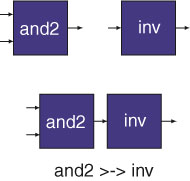
An example of serial composition is shown below for the circuit and2 >-> inv. The circuit and2 takes a pair of signals as its input and returns a single output bit. This is illustrated in the diagram below:
The and2 circuit is realized in a two-sided Lava tile which means that signals (either inputs or outputs) can occur on the left or right hand sides of the tile but not the top or bottom. The inv circuit is also realized in a two-sided tile. To make an NAND gate form these components all one needs to do is to connect the output of one circuit to the input of the other circuit. This task can be performed by the serial composition combinator without having to name the intermediate signals.
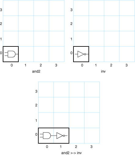
However the serial composition combinator does more than just connect wires together. Serial composition looks at the sizes of the circuits it has to compose and it lays out one circuit directly next to the other circuit with their bottoms aligned. For example consider the tiles containing the inv and and2 gates which which each have size (1,1). The serial composition combinator takes the output of the and2 gate and connects it to the input of the inv gate resulting in a circuit that behaves like a NAND-gate. It also places the inv gate to the right of the and2 gate so it ends up in location (1,0). The composite NAND-gate circuit tile has size (2,1) as shown below.
The and2 gate at Lava location (0,0) has been mapped into the upper LUT of the left hand slice of the CLB at R32C1 i.e. R32C1.S1 (the left hand corner of this Virtex device). The inv component has been mapped into the upper LUT of the right hand slice in the same CLB i.e. R32C1.S0. Note that within the slice the Xilinx tools are free to map to either the upper or lower LUT (F or G). Lava coordinates can specify which logic should be mapped into a slice by requesting either F (y coordinate an even number) or G (y coordinate an odd number) in a relative coordinate system but the Xilinx mapper will decide the actual mapping and absolute location. For the Virtex-II architecture Lava generates slice-based coordinates.
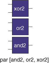
The serial composition combinator is useful when we wish to compose and lay out two circuits that communicate. Sometimes however we wish to lay out circuits relative to each other which do not communication. One of the many combinators that Lava provides for composing circuits in parallel is the par2 combinator. This combinator takes two two sided tiles and placed the second tile above the first tile aligned along their left hand edges. An example layout for the circuit par2 inv and2 is shown below:
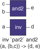
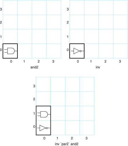
Any circuit or combinator that takes two inputs can be written as in infix operator in Lava by enclosing the name of the circuit or combinator in back quotes as shown above i.e. par2 inv and2 is the same as inv `par2` and2. The par2 combinator produces a composite circuit that takes a two element tuple as its input and returns a two element tuple. The first element of the input tuple is the input destined for the first (lower) circuit and the second element of the input tuple is the input destined for the second (upper) circuit. The first element of the output tuple is the output from the first (lower) circuit and the second element of the output tuple is the output from the second (upper) circuit. The layout of the composite circuit tile of size (1,2) in the Lava coordinate system is shown below.
The par2 combinator operates over just two circuits. Three or more circuits can be composed by using par2 as an infix operator but this results in circuits with awkward tuple types. The par combinator takes a list of circuits (all of the same type) and lays them out from the bottom to the top:
Sometimes it is useful to apply the same circuit to every element of an input bus. We can use the Haskell higher order map function and the Lava par combinator to define a circuit combinator which performs exactly this task. The Lava combinator that maps a circuit across a bus is called maP (with a capital P to it does not clash with the Haskell function map) and is defined as:
maP r = par (repeat r)
This combinator takes any circuit r (which is considered to be a two sided tile) and replicates it as many times as there are elements in the input bus and then layouts out these replicated circuits vertically. For example to invert every bit on a bus one would write maP inv resulting in the layout shown below:

Another use of maP is to vertically place registers across each element of a bus. The basic register in Lava that corresponds to FD takes two inputs: the clock and the D input signal. The circuit vreg registers each element of a bus and is define as:
vreg clk = maP (fd clk)
A register fits in a tile of size (1,1). To describe an AND gate with a register at the output we could use serial composition:
and2Reg clk = and2 >-> fd clk
This produces the following layout:
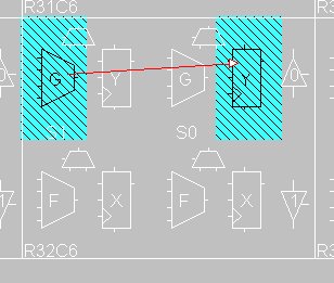
Why is the register realized in the adjacent slice and not the slice containing the function generator for the AND2 gate? This is because the and2 circuit occupies a tile of size (1,1) and the register also occupies a tile of size (1,1) and when the serial composition combinator is asked to put one tile next to the other that is exactly what it does. This results in the register being realized in location (1,0). If this is not what is wanted then a variant of the serial composition combinator can be used to compose two circuits without translating the second circuit. This combinator is called the serial overlay combinator and is written as >|>. The circuit and2 >|> fd clk will realize both the and2 circuit and the inv circuit into location (0,0) giving:
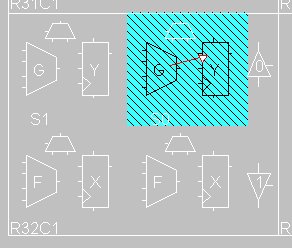
Now the and2 gate and the FD register are realized in the top half of one slice. Lava will always map and place circuits exactly in the way specified by the layout combinators.
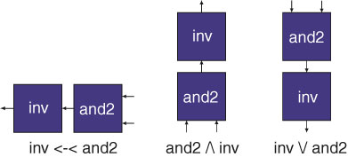
The >-> serial composition combinator only composes circuits with a left to right data-flow. There are three other serial compositions combinators that describe right to left (<-<), bottom to top (/\) and top to bottom (\/) serial composition. They are illustrated below:
To describe circuits that communicate on more than two faces of a tile Lava also provides support for four sided tiles. A circuit can be put inside a four sided tile if it has a type which takes a two element tuple as its input and returns a two element tuple as shown below
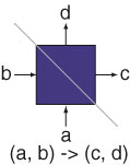
A four sided tile is divided into the input signal and output signal portions by the gray diagonal line. The input to a circuit that fits into a four sided tile must be a tuple (a, b) where the a signal is connected to the bottom of the tile and the b signal is connected to the left of the tile. These signals can be single bits or composite signals. The result type of a circuit that fits into a four sided tile must also be a tuple (c, d) where the c signal is connected to the right hand side of the tile and the d signal is connected to the top of the tile.
To put one four sided tile below another four sided tile requires a new combinator because these tiles do not have the appropriate types for the par2 combinator. Lava provides the below combinator for this task and the picture below shows the circuit r `below` s:
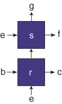
The circuit r has the type (e,b) -> (c, x) and the circuit s has the type (x,e) -> (f, g) and the composite circuit has the type (e, (b, e)) -> ((c, f), g) where x is the type of the intermediate signal that r and s communicate along. There is also a beside combinator that lays out s to the right of r.
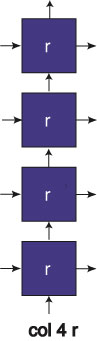
Four sided tiles can be replicated and composed to form columns and rows. The col combinator tiles a circuit r vertically and forms connections between the top and bottom faces of the tile:
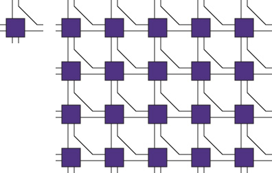
The row combinator composes tiles horizontally from left to right and is based on the beside combinator. Rows and column combinators can be used to describe many interesting layout patterns and emulate layout grids which are not four sided. Here is how a hex-connected grid might be described in terms of four sided tiles:
Next section: An Adder Example